N-channel MOSFET
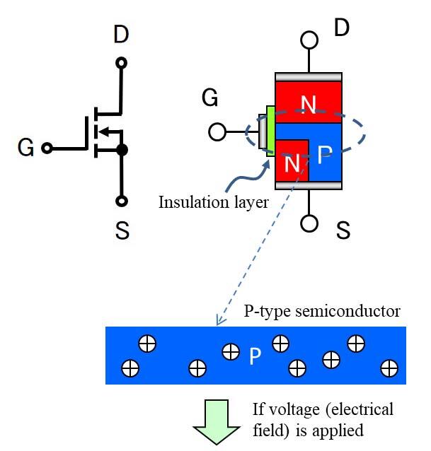
The route between D→S is N→P→N and the N→P junction is backwards, so current cannot flow.
There are + electrical charges called “holes” distributed across P-type semiconductors.
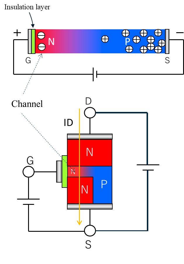
If voltage is applied between G-S, the P layer directly below the gate will invert to N, creating an N-type semiconductor layer.This changes the N→P→N route to N→N→N, allowing current ID to flow.
This is a MOSFET in the “ON state”.
This N-type layer is called a “channel”, and because the channel is N-type, this is called an “N-channel MOSFET”.
The resistance of the channel is called the “channel resistance”.
MOSFET gate threshold value (P8FE10SBK example)
|
Item |
Rating |
Unit | Explanation | ||
|---|---|---|---|---|---|
|
Min. |
Typ. | Max. | |||
|
VTH |
1.5 |
2.0 |
2.5 |
V |
Voltage between G-S at which ID begins to flow (turns ON) |
① VGS=1V
Even if 1 V of voltage is applied between G-S, the channel will remain P and no current will flow.
② VGS=2V
If approximately 2 V of voltage is applied between G-S, then the channel will invert to N and current will begin to flow. ⇒This is the threshold value (VTH)
③ VGS=4.5V
In order to reliably lower the ON resistance, a voltage which is sufficiently larger than the VTH must be applied.
VGS = 85 mΩ at 4.5 V, VGS = 79 mΩ at 10 V
Body diode
As shown in the figure, the area between S⇒D is already a PN junction, or a diode, so current can flow at anytime.
This diode is called a “body diode”, and the MOSFET symbols are also written as shown in the figure.
P-channel MOSFET
The route between S→D is P→N→P and the N→P junction is backwards, so current cannot flow.
If voltage is applied between G-S, the N layer directly below the gate will invert to P, creating an P-type semiconductor layer (channel).
This changes the P→N→P route to P→P→P, allowing current ID to flow.
This is a MOSFET in the “ON state”.
The channel is P-type, so this is called a P-channel MOSFET.
Because the current in P-type semiconductors is carried by “holes”, it is more difficult for current to flow in P-type semiconductors than in N-type semiconductors where current is carried by “electrons”.
In short, for the same size chip, the resistance will be higher than in an N-type.
P-channel MOSFET characteristics
- Negative voltage is applied between G-S to turn ON the MOSFET.
- Has higher ON resistance than N-channel MOSFET.
- The body diode is D→S orientation.
Due to these characteristics and from a usability standpoint, the majority of MOSFET used in the marketplace are N-channel MOSFET, and the product lineups of semiconductor manufacturers overwhelmingly feature N-channel MOSFET.
-
-

- P-Channel
-
P-channel MOSFET usage examples
-
-

- Step-down DC/DC converters
-
-
-

- Low loss conversion of reverse battery protection diodes
-
